Scanning Microwave Microscopy Option

Nanosurf's SMM Option is the fast and user-friendly solution for performing electrical characterization of dielectrics, semiconductors and metals with high sensitivity.

It is quick to set up, easy to learn and only minimal sample preparation is needed. 

  • Fastest path to your SMM characterization
  • Set up in 3 clicks
  • Developed by Nanosurf: both AFM and SMM

An added benefit of Nanosurf's SMM solution is that both the AFM and SMM technology were developed at Nanosurf - resulting in better compatibility and improved customer support. 

Example measurements

SMM on SRAM sample
Topography (left), Im(S11) or capacitance (right) of an SRAM sample. Scan size is 25 x 25 μm2.
SRAM sample
Topography (left), Im(S11) or capacitance (right) of an SRAM sample. Scan size is 10 x 10 μm2.
Amplitude and phase SRAM sample
Amplitude of dS/dV (dC/dV) measurement (left), and phase (right) of an SRAM sample. Scan size is 11 x 11 μm2.
MC2 capacitance standard sample
Topography (left), capacitance map in fF (middle) of an MC2 capacitance standard sample – gold dots on SiO2 terraces on Si. The dotted line on the capacitance map denotes the area of the cross-section on the right. The smallest capacitance of a dot is 0.3 fF and capacitance steps between terraces are 0.04 fF. Scan size is 52 x 52 μm2.
SCM calibration sample
Topography (left), S11 amplitude (middle) and dopant density map (right) of an Infineon SCM calibration sample with dopant densities in a range of 4x10¹⁵ – 1020 cm-3. Scan size is 50 x 50 μm2.
Infineon SCM sample
Amplitude of dS/dV (dC/dV) measurement (left), and phase (right) of an Infineon SCM sample. Phase image shows clear difference between doping types: N or P. Scan size is 40 x 40 μm2.

Software - set up in 3 clicks

smm_gui

The uncluttered Nanosurf SMM GUI is intuitive to use and focuses on what's important: system controls (left) and scan window (right). A measurement can be set up and run with only a few clicks.

What is SMM?

Scanning microwave microscopy (SMM) is a scanning probe technique, that measures the interactions of a microwave from a sharp tip with the sample. The microwave reflection coefficient (S11 parameter), which is the ratio between the microwave power sent to the tip and the one received back after being reflected at the tip-sample contact, is used to deduce the local tip-sample microwave impedance. The microwave impedance yields information about the local capacitance from which one can deduce the dielectric constant and the dopant density. In terms of the dopant density measurement, SMM is similar to scanning capacitance microscopy (SCM), but offers wider range of measurements. SMM can be used for measurements of not only semiconductors, but also dielectric materials and metals, since it is not solely relying of the modulation of the depletion capacitance in the sample.

SMM at a glance

  • Electrical characterization of materials – dielectrics, semiconductors and metals
  • High sensitivity to changes of dopant density in semiconductors
  • High sensitivity to DC capacitance
  • Minimal sample preparation
  • Imaging of buried structures
smm_controller
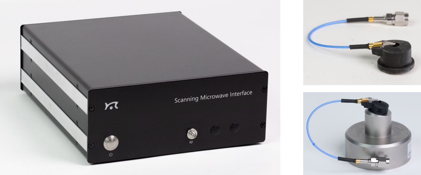
Nanosurf SMM controller (left), SMM cantilever holders: DriveAFM (top right), FlexAFM (bottom right).

Understanding the S11 Parameter

The S11 parameter is defined as a function of the complex impedances of reference impedance (Z0) and load (ZL) – Eq.1. Impedance is a complex value and can be represented as a sum of real and imaginary parts – Eq.2. The real part of Z is resistance (R) and the imaginary part can be considered as capacitance (C) -Eq.3. Depending on the sample, resistance and capacitance are functions of conductivity, dielectric constant and carrier density.

smm_equations

Hardware

Powerful digital signal processing is analysing signal at 1 MHz, far away in frequency from 1/f noise. The signal is digitized early at the analog front-end and such typical issues of analog systems as DC-offset re-adjustment are absent in this configuration. FPGA software has sideband detection capabilities, and dS/dV (dC/dV) measurement does not require any additional hardware, e.g. lock-in amplifiers. Both S11 and dS/dV signals are digital. High working frequency around 5 GHz means better sensitivity to capacitance.

smm_hardware

Block diagram of the Nanosurf SMM electronics.

Webinar: Scanning Microwave Microscopy

In this webinar, Dr. Denis Vasyukov shows how Scanning Microwave Microscopy works theoretically, and how this mode of measurement performs on Nanosurf instrumentation. The webinar is aimed at novice and advanced AFM users.

Application notes and detailed technical explanation

SMM enables the precise measurement of local capacitances with exceptional sensitivity, providing crucial material and device parameters essential for the thorough characterization of semiconductor materials and electronic structures. This selection of application notes offers a detailed description of the measurement process and technology, along with numerous examples of its applications.

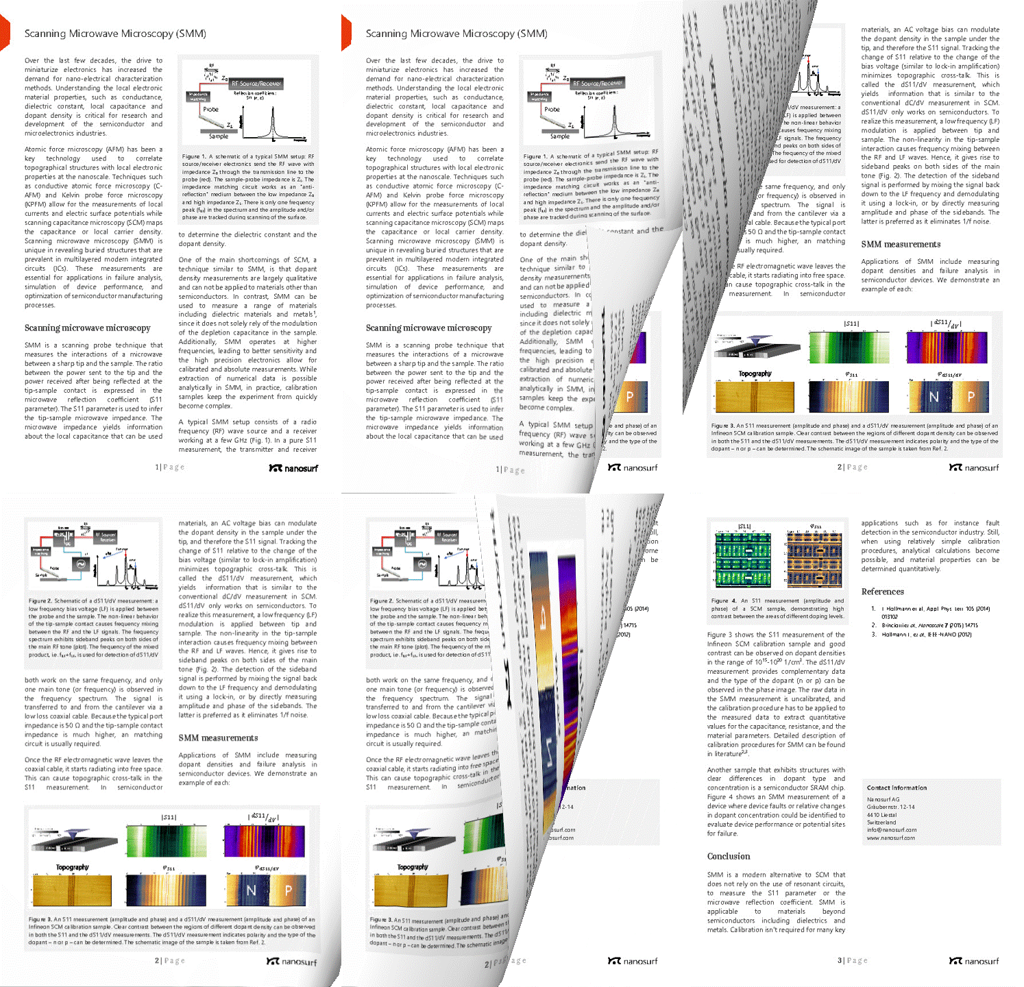
Thunmbnail-SMM

Technical note:
Scanning Microwave Microscopy

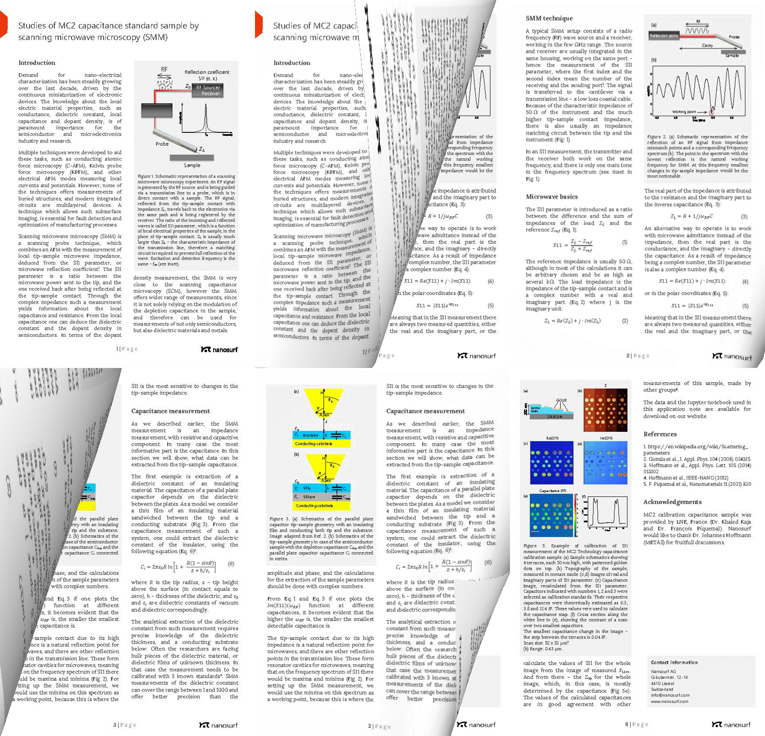
Thunmbnail SMM MC2 capacitance

Studies of MC2 capacitance standard sample by scanning microwave microscopy

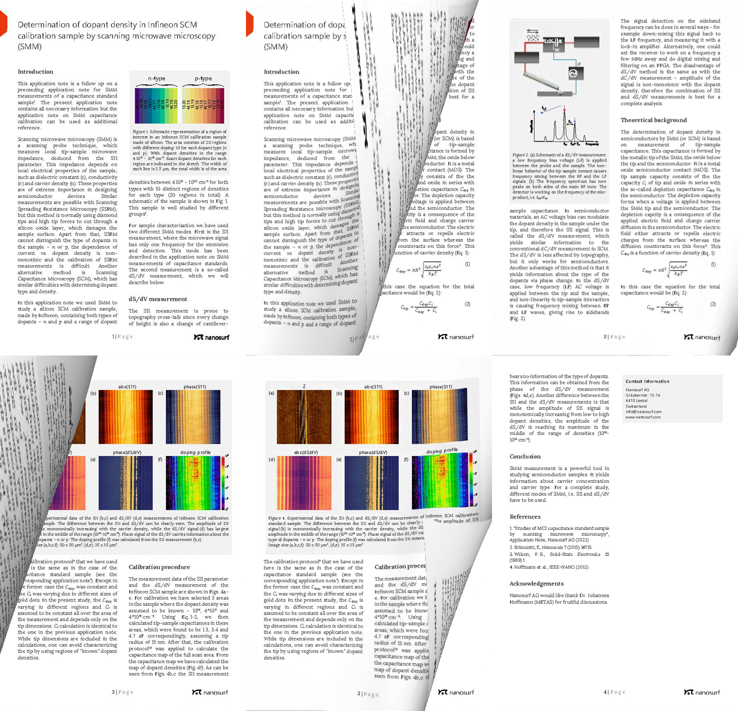
SMM dopant density

Determination of dopant density in Infineon SCM calibration sample by scanning microwave microscopy 

SMM Semicon tech note

Scanning Microwave Miscroscopy for the Semiconductor Industry

SMM option brochure download

SMM_brochure_cover
DriveAFM-black-1

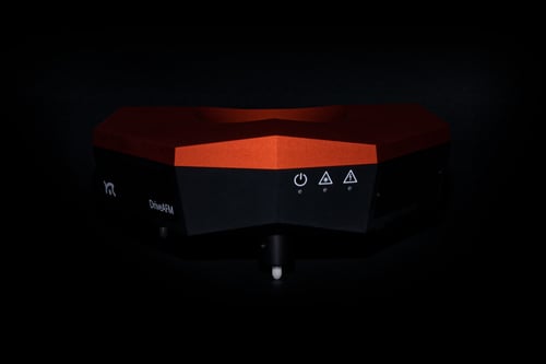
DriveAFM

The flagship AFM by Nanosurf that leaves nothing to be desired:

  • Fast
  • Intuitive
  • Performance without compromise
FlexAFM-black

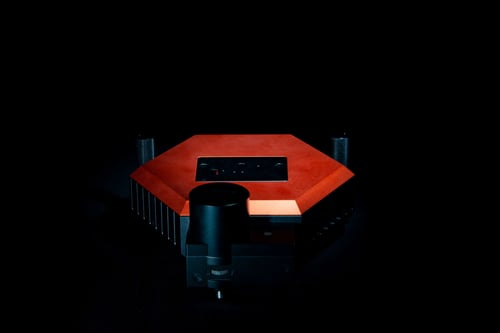
FlexAFM 

The most flexibly configurable AFM for materials and life science research:

  • Our mid-range allround instrument
  • One of the most established AFMs available
  • Built-in upgrade path to DriveAFM
CoreAFM

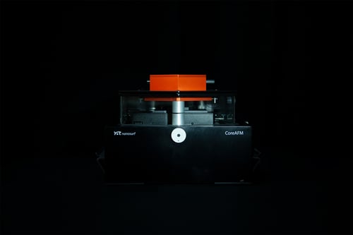
CoreAFM

AFM for multi-user settings and sophisticated education:

  • Allround AFM with a competitive price tag
  • 33 modes and functions out of the box
  • Easiest AFM to handle with confidence