Discover how Nanosurf's collaboration with a team of scientists has revolutionized spring constant calibration for ...
03.11.2023

Héctor here, your AFM expert at Nanosurf calling out for people to share their Friday afternoon experiments. Today I'll introduce you to the nanoscale part of the Coherer effect.
What is the Coherer effect?
In short, the Coherer is like a very basic transistor (in fact it is considered the first memristor, see Ref 1) consisting of two electrodes with metal particles in between. In its normal state there is no electrical conduction, but when it is shaken or a high voltage appears, it starts conducting electricity and remains conducting it until you shake again the particles. The behaviour of the metal particles is what some people refer to as Coherer effect.
My not so good explanation: Some metals (e.g. aluminum) have an external oxide layer that prevents corrosion to take over the whole material and at the same time prevents electrical conduction. This oxide layer is so thin, that even an small pressure (or some large voltage) can break it, creating a channel for electricity to flow. This is what opens or closes the conduction between the two electrodes of the Coherer device.
Mehdi more fun and interesting experiment/explanation:
(By the way, Mehdi, I do hope this post makes its way to you, because I'm a big fan of yours and enjoy every single one of your publications).
So, the question now for us is, can we measure the thickness of the oxide layer in aluminum?
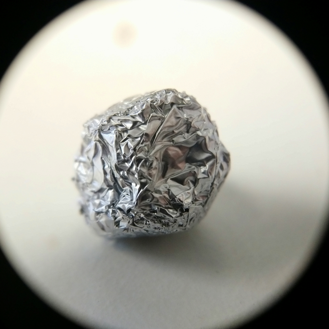
For this experiment I use kitchen foil (the not shiny side), and diamond probes from Adama Innovations (AD 40 because I don't know how thick or how difficult will be to pierce the oxide, so I start in the middle of the range they offer). The diamond part will minimize the probe degradation when doing a lot of indentation measurements, so in principle it should be easier to compare results.
This below is how kitchen foil looks like, topography on the left and current map on the right. In this case, the probe was biased with 5 V (which is good to image, because, as we will see later, should induce conduction with very small applied force).
My next step was to perform a lot of indentation curves with different applied voltages to see at which depth of the indentation current starts to flow between the probe and the conductive substrate.
So, two things.
First a brief explanation of indentation curves. What you see below is probe deflection and electrical current as the probe approaches the surface and pierces through the oxide layer (with 3V between the probe and the aluminum substrate). At the beginning deflection is flat and current is zero because the probe is far away from the surface. At some point there is a pull form the surface because the water, that covers everything in air, forms a meniscus (there is also the effect of the electrostatic field, but as you will see later, this is likely to be much smaller as its variation with the applied voltage cannot be easily noticed). After the meniscus is formed, at some point the probe starts indenting the oxide layer and the deflection starts increasing. After about 50 nm current increases in a short of telegraphic noise fasion, this is because we are close to the limit where conduction happens. Then, after about 150 nm conduction is stable and we have definitely pierced through the oxide layer (i.e. the combination of distance and voltage is such that electrons can pass from the probe to the aluminum). So, is 150 nm the thickness of the oxide layer? No. Because we were applying a voltage, conduction happens at much shorter distance, because the voltage induces it. The thickness of the oxide layer, the real thickness, will be the one measured without applying a voltage. Unfortunately, if we don't apply a voltage we cannot generate a current, thus the only solution is to measure the breakdown distance with different applied voltages and then extrapolate what is the thickness.
Second. We want to measure many indentation curves and process them. Also, we want the curves to be taken in random places to avoid damaging an area of the aluminum and thus obtaining an artificial result, so we need to choose the position of the indentation randomly. For this reasons is why I made these two python codes below. The first one is to do the indentation. One should open Nanosurf CX software, approach the surface, take a reference image, and then setup the spectroscopy to do a force-distance ramp, then run the script which will take over choosing different points in the surface, adjusting the voltage and saving the data.
import nanosurf
import time
import numpy as np

#Some constants
maxV=-5
Vstart=0
V=Vstart
steps=25
repetitions=3

#Initilaize connection to AFM system
spm = nanosurf.SPM()
application = spm.application
scan = application.Scan
stage = application.Stage
application.AutoExit = False
spec = application.Spec
ZCtrl = application.ZController

#Probe retracted when moving from one indentation site to another, and voltage set to initial voltage.
application.system.SystemStateIdleZAxisMode=0
ZCtrl.TipVoltage = Vstart

#Asumes the AFM system is approached to the surface and spectroscopy parameters set
#Loop through voltages. At each voltage moves the tip to a random position and performs an indentation
for t in range(steps):
    V=(maxV-Vstart)/steps*t+Vstart
    ZCtrl.TipVoltage = V
    for m in range(repetitions):
        spec.ClearPositionList()
        x=np.random.random()*100e-6-50e-6
        y=np.random.random()*100e-6-50e-6
        spec.AddPosition(x, y, 0)
        application.SetGalleryHistoryFilenameMask("Voltage_"+str(V)+"_[INDEX]")
        spec.Start()
        #While the AFM indents, the script waits
        while spec.IsMeasuring == True:
            time.sleep(10)
            print("measuring")
Then, to analyze the data I used this bit of code below which opens the *.nid files and extracts the deflection and current data.
from NSFopen.read import read
import numpy as np
import matplotlib.pyplot as plt
from pathlib import Path
import tkinter as tk
from tkinter import filedialog

#GUI to select the datafile
root = tk.Tk()
root.withdraw()
filename = filedialog.askopenfilename()
name=Path(filename).stem

# Read *.nid data format
afm = read(filename, verbose=False)
data = afm.data # Data
param = afm.param # AFM parameters
#Not used, but as an example of how to get data.
k = param.Tip.Prop0['Value']  # spring constant
sens = param.Tip.Sensitivity['Value']  # deflection sensitivity (if needed)
z=data['Spec']['Forward']['Z-AxisSensor']# Z-axis data
y1=data['Spec']['Forward']['Tip current_AUX']
y2=data['Spec']['Forward']['Deflection']

#Baseline correction
slope1=(y1[0][100]-y1[0][0])/(z[0][100]-z[0][0])
y1[0]=y1[0]-slope1*z[0] #First subtract slope based on a basic slope
y1[0]=y1[0]-y1[0][0] #Subtract offset

slope2=(y2[0][2000]-y2[0][0])/(z[0][2000]-z[0][0])
a=np.average(y2[0][2000:3000])
b=np.average(y2[0][0:2000])
slope2=(a-b)/(z[0][2500]-z[0][1000])
y2[0]=y2[0]-slope2*z[0] #First subtract slope based on a basic slope
y2[0]=y2[0]-y2[0][0] #Subtract offset

#Height correction
zeroindex=np.max(np.where(y2[0] == np.min(y2[0])))
z[0]=z[0]-z[0][zeroindex] #Match beginning of indentation with distance to sample=0

#Plotting the data with dual axis
COLOR_current = "#69b3a2"
COLOR_deflection = "#3399e6"
fig, ax1 = plt.subplots()
ax2 = ax1.twinx()
ax1.plot(z[0]*1e9, y1[0]*1e9,color=COLOR_current, lw=3)
ax2.plot(z[0]*1e9, y2[0],color=COLOR_deflection, lw=4)
ax1.set_xlabel("Z-axis [nm]")
ax1.set_ylabel("Current [nA]", color=COLOR_current, fontsize=14)
ax1.tick_params(axis="y", labelcolor=COLOR_current)
ax2.set_ylabel("Deflection [V]", color=COLOR_deflection, fontsize=14)
ax2.tick_params(axis="y", labelcolor=COLOR_deflection)
ax1.set_xlim(-500,500)
ax1.set_ylim(-2,27)
ax2.set_ylim(-0.3e-6,6e-6)

#Saving as an image
fig.savefig(name+".png")
#Saving as CSV
x=np.zeros([len(z[0]),3])
x[:,0]=z[0][0:len(z[0])]
x[:,1]=y1[0][0:len(z[0])]
x[:,2]=y2[0][0:len(z[0])]
np.savetxt(name+"data.txt", x,delimiter=',',fmt='%e')
The results when running both scripts and performing the measurements are something like this:
Which is pretty cool because we can see how the point where the current starts to pass moves closer and closer to the moment the probe starts indenting the surface, indicating that increasing the voltage helps creating the electrical connection.
We can also see the noise due to false connection that appears sometimes, this is why for each voltage I repeated the measurement several times and (to save myself time and calculations), plot only the most representative curves.
So, time to answer the question, does the data make sense? Can we say what is the thickness of the oxide layer? Judge by yourselves.
We obtained an oxide thickness of about 307 nm, which is a reasonable value, and a breakdown voltage of about 5.6 V (this is not very representative, because it is the voltage that the electric field from the sharp tip needs to pierce the oxide, a probe with different geometry will need a slightly different voltage, but it is still interesting to know.
Final remarks: When moving the tip from one position to another it is important to retract from the surface, otherwise you might be scratching it and altering the results. Similarly for voltage, if you arrive to a new probe location with a high voltage and lower the voltage afterwards, you very likely already modified the surface and your results will be biased.
I hope you find it useful, entertaining, and if you are Mehdi and you read this far, thank you for the inspiration, really appreciate your work. Please (every one now) let me know if you use some of this, and as usual, if you have suggestions or requests, don't hesitate to contact me.
Further reading/references:
1 G. Gandhi, V. Aggarwal and L. Chua, "Coherer is the elusive memristor," 2014 IEEE International Symposium on Circuits and Systems (ISCAS), Melbourne, VIC, Australia, 2014, pp. 2245-2248, https://ieeexplore.ieee.org/document/6865617
2 Conductive AFM: https://www.nanosurf.com/en/support/afm-modes-overview/conductive-afm-c-afm
3 Force spectroscopy: https://www.nanosurf.com/en/support/afm-modes-overview/force-spectroscopy
29.11.2023
Discover how Nanosurf's collaboration with a team of scientists has revolutionized spring constant calibration for ...

01.11.2023
Discover the advanced applications of electrical Atomic Force Microscopy in this white paper. Learn about electrical ...

01.11.2023
Nanosurf | AFM Knowledge Discover the importance of calibration samples in AFM and how they contribute to ...

09.05.2024
FridayAFM: Want to study pollen? Here are some tips and tricks to prepare samples for AFM imaging.

02.05.2024
FridayAFM: Want to study pollen? Here are some tips and tricks to prepare samples for AFM imaging.

23.04.2024
FridayAFM: See how the stiffness varies across the cells forming part of the lettuce stomas.
Interested in learning more? If you have any questions, please reach out to us, and speak to an AFM expert.