See our example applications for a glimpse of the possibilities AFM offers you.
See our example applications for a glimpse of the possibilities AFM offers you.
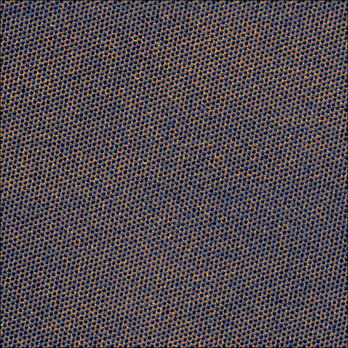
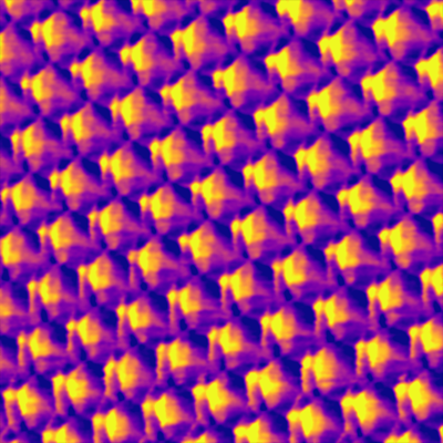
hBN on graphene moiré superlattice revealed by photothermal torsional resonance imaging
Torsional resonance phase image of hexagonally packed boron nitride on graphene with a 2.2° twist between the layers showing a moiré superlattice. Torsional resonance was photothermally excited using CleanDrive. Photothermal torsonal resonance imaging provides another possibility to reveal moiré patterns without the need for any kind of electrical excitation. Image size 500 nm, color scale 9.6°.

-and-1.jpg?width=400&height=400&name=AN01294_twisted-graphene-on-hBN_PFM_2D_153-nm-xy_-35-pm(amplitude%2c-left)-and-1.jpg "AN01294_twisted-graphene-on-hBN_PFM_2D_153-nm-xy_-35-pm(amplitude,-left)-and-1")


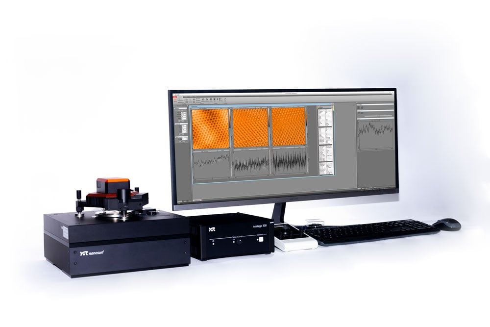
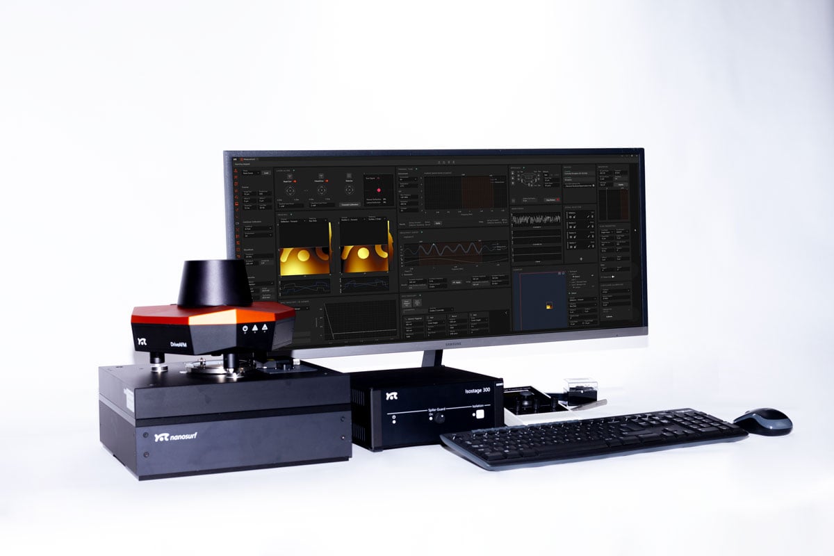
Drive AFM
Nanosurf's flagship AFM system delivers ultimate performance for your 2D materials research. If you want performance without compromise, the DriveAFM is the instrument of choice.
- Resolve atomic lattice and moiré patterns simultaneously
- Ultra-low noise
- High stability thanks to CleanDrive
- Glovebox compatible
FlexAFM
Nanosurf's FlexAFM is one of the most established research AFMs available. Famous for its ease of use, this instrument excels in the glovebox and at applications involving electrical characterization.
- Versatile allround AFM system
- Large selection of electrical modes
- Established research AFM with unparalleled value
- Popular glovebox AFM